
Optical Coatings
Precision thin-film optics for photonics, defense, and consumer devices
PVD deposition — primarily magnetron sputtering and electron beam evaporation — enables the precise, multi-layer optical stacks required for anti-reflection, high-reflection, bandpass, beamsplitter, and specialty filter coatings across UV, visible, and infrared wavelength ranges.
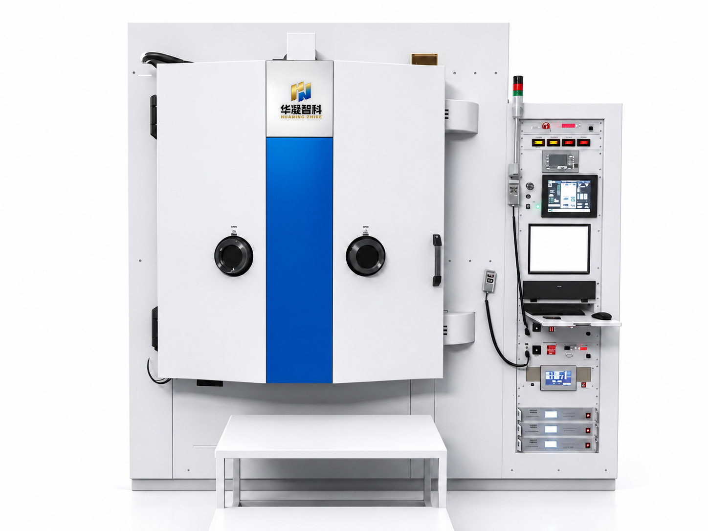
Overview
Optical coating is one of the most precision-demanding applications of PVD technology. Achieving target reflectance or transmittance spectra requires exact control of layer thickness (often to sub-nanometer accuracy), refractive index, and surface roughness across multilayer stacks that may comprise dozens of individual layers. HUANING ZHIKE systems support the full range of optical thin-film work — from laboratory feasibility studies to production-scale coating of lenses, mirrors, filters, and photonic components.
Application Areas
Anti-Reflection (AR) Coatings
Reduce reflection losses on optical lenses, display panels, and solar cells across broadband or targeted wavelength ranges.
High-Reflection (HR) Mirrors
Near-unity reflectance mirrors for laser cavities, telescope optics, and precision measurement instruments.
Bandpass and Notch Filters
Narrow spectral selection for fluorescence microscopy, lidar, spectroscopy, and laser line isolation.
Beamsplitters
Precise reflectance/transmittance ratios for interferometry, imaging, and optical measurement.
Infrared Optical Coatings
Coatings on germanium, ZnSe, and chalcogenide substrates for thermal imaging and defense optics.
Transparent Conductive Oxides
ITO and AZO films for display touch panels, photovoltaic cells, and electrochromic devices.
Applicable Deposition Methods
Electron Beam Evaporation — preferred for highest-purity dielectric and metal layer deposition; excellent layer-by-layer thickness control via QCM and optical monitoring
Magnetron Sputtering — enables reactive deposition of oxide and nitride layers with excellent lateral uniformity; suited for large-area optical production
Magnetron & Electron Beam Composite — combines strengths of both methods for complex stacks requiring both high-purity evaporation and reactive sputtering layers
Key Process Considerations
In-situ optical broadband monitoring or QCM for precise layer thickness control
Planetary substrate rotation for large-area uniformity
Clean UHV or high-vacuum environment to minimize contamination
Ion-assist deposition capability for dense, low-scatter films at reduced temperature
Multi-material hearth or multi-target carousel for sequential stack deposition without air breaks