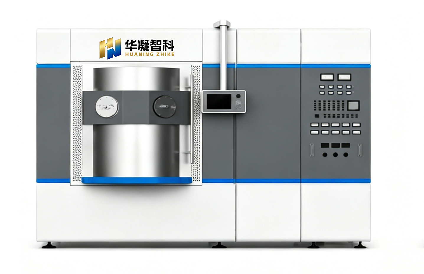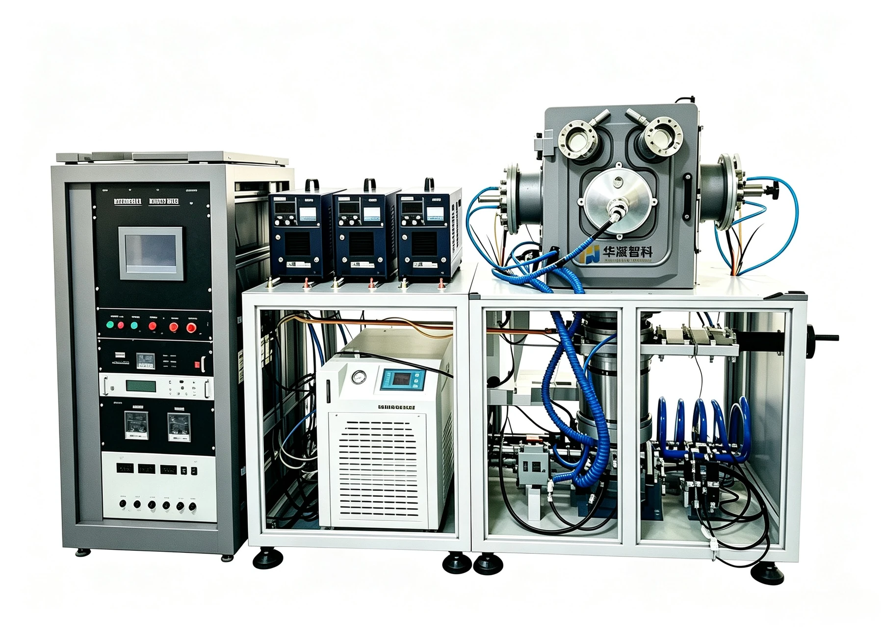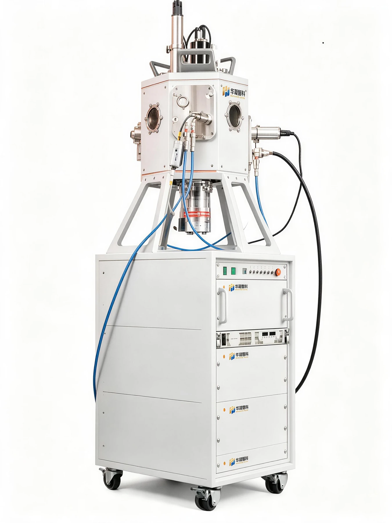
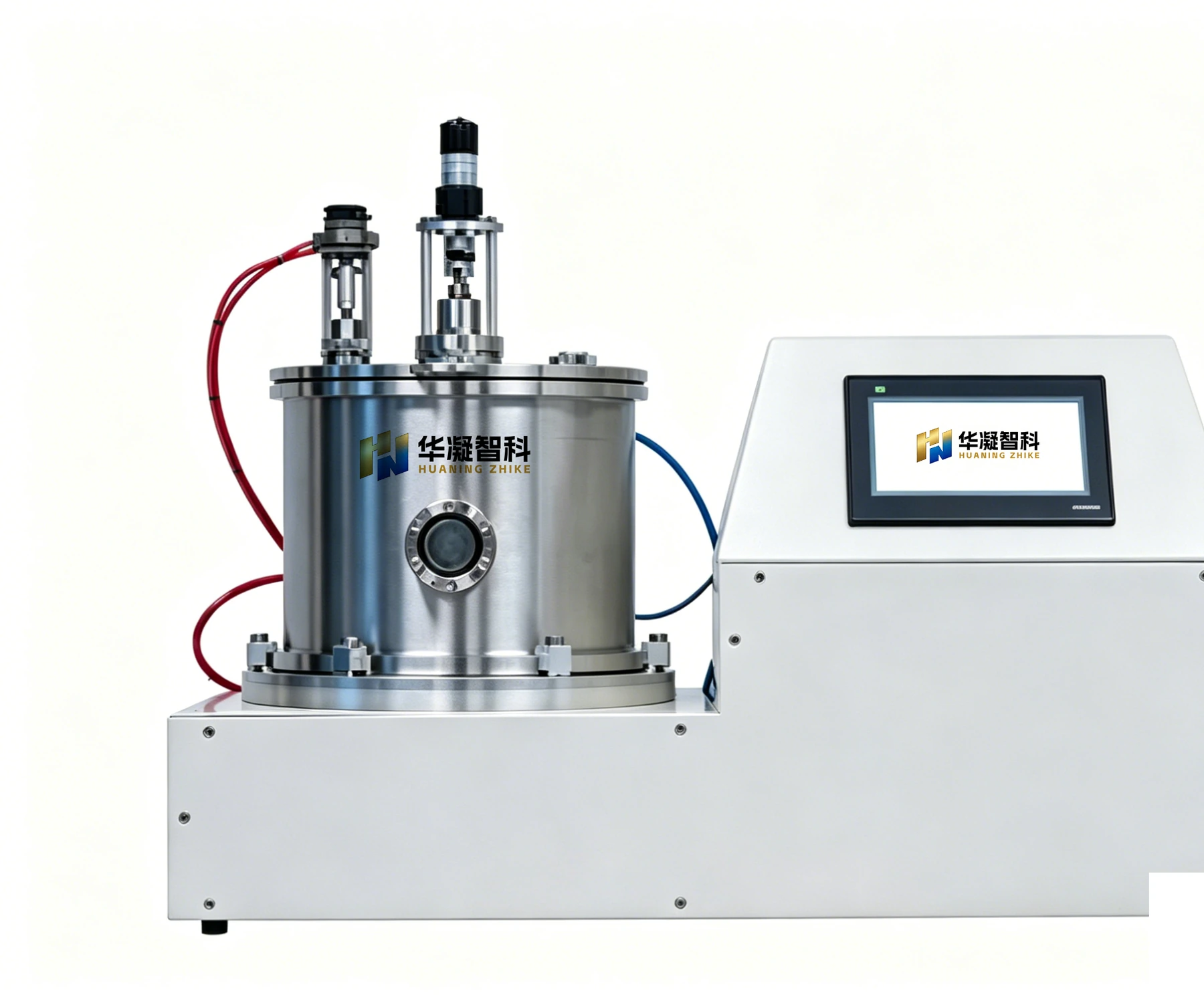
Small Magnetron Sputtering R&D Equipment
Precision research sputtering with full parameter accessibility
System Overview
The HN-MS-R-007 is a research-grade magnetron sputtering platform built for thin-film research and process development in academic, semiconductor, and optical technology laboratories. Supporting multiple sputtering configurations — including co-sputtering and sequential deposition — the system provides the parameter range and in-situ measurement options expected of a premier research tool.
Working Principle
Planar or confocal magnetron sputtering sources enable DC, RF, and pulsed-DC operation across a wide range of metallic, ceramic, and compound target materials. The research-oriented design prioritizes measurement access, flexible geometry, and compatibility with analytical instruments.
Core Advantages
- Multi-target configuration for co-sputtering and alloy film development
- DC, RF, and pulsed-DC source options for conductive and insulating targets
- Configurable monitoring interfaces defined during system engineering
- UHV-compatible chamber design for contamination-sensitive research
- Wide-range substrate temperature control from ambient to 1200 °C with in-situ annealing
- Multiple gas inlet channels for reactive and mixed-atmosphere studies
- Integrated in-situ ion cleaning for substrate preparation
- Compatible with wafers up to 8 inches and small research samples
Technical Specifications
| Chamber | φ400/500 mm chamber |
|---|---|
| Targets | 2–4 planar magnetron targets with DC/RF power |
| Power Control | Independent target power adjustment with co-sputtering support |
| Temperature Control | Wide-range substrate temperature control from ambient to 1200 °C with in-situ annealing |
| Substrate Preparation | Integrated in-situ ion cleaning for substrate surface activation before deposition |
| Sample Compatibility | Wafers up to 8 inches and small research samples or coupons |
| Thickness Monitoring | Real-time QCM thickness recording |
| Data System | Independent sample records with one-click experiment-curve export |
Specifications are representative. Final system parameters are defined during configuration. Contact our engineering team for detailed documentation.