Magnetron & Electron Beam Integrated Research Platform
Advanced research platform integrating sputtering and evaporation
System Overview
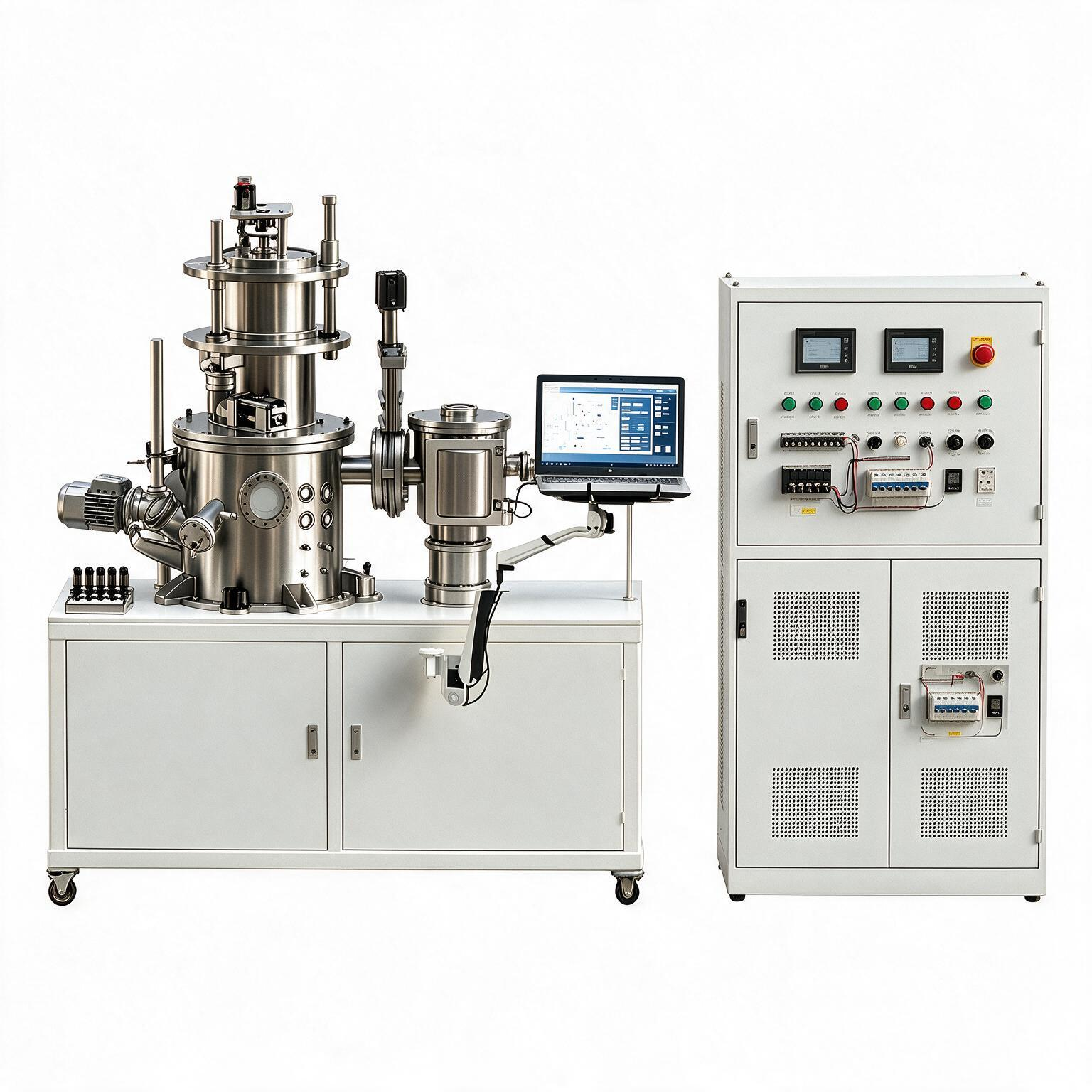
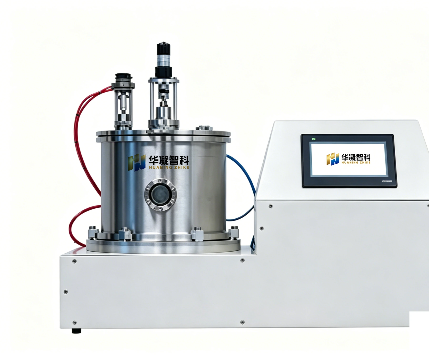
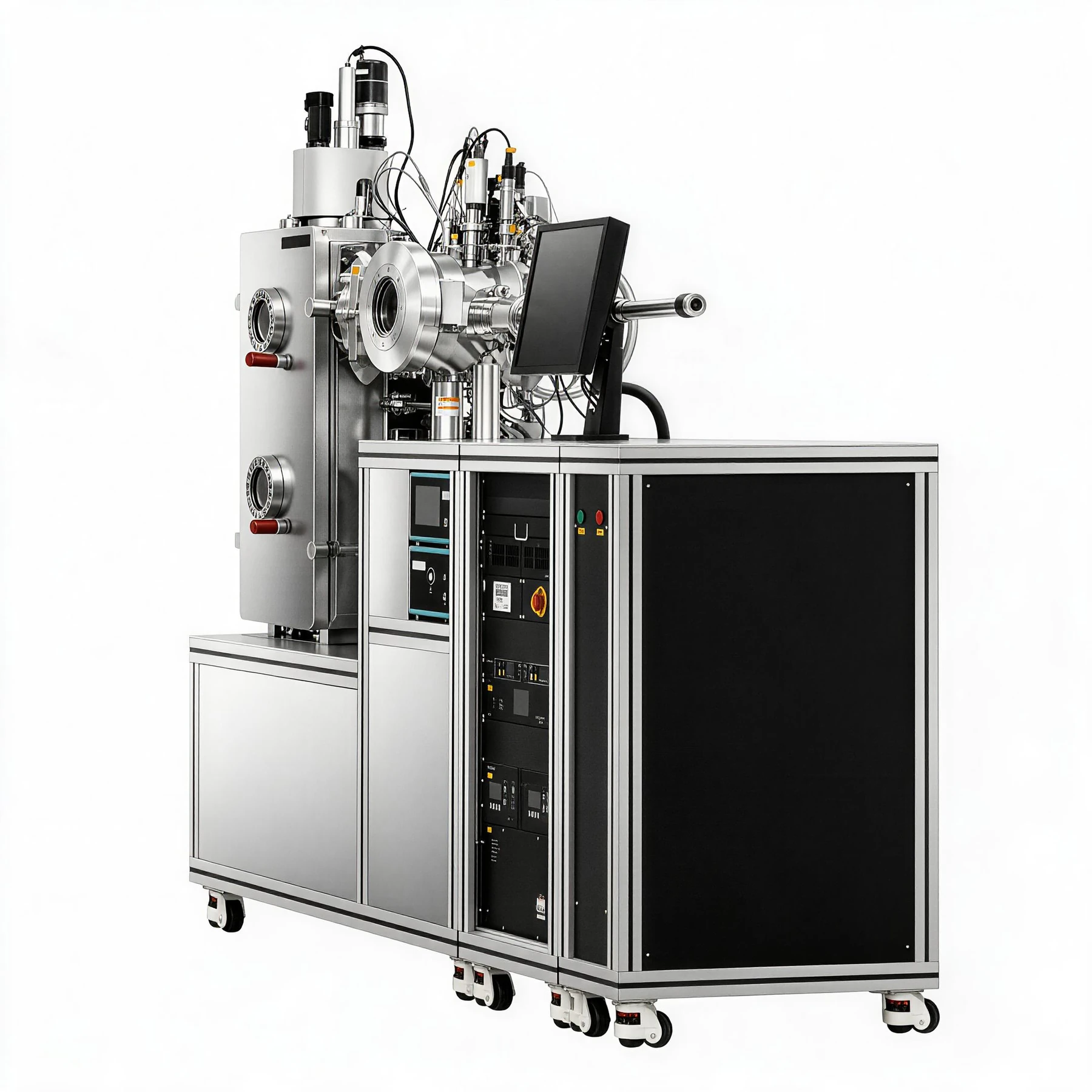
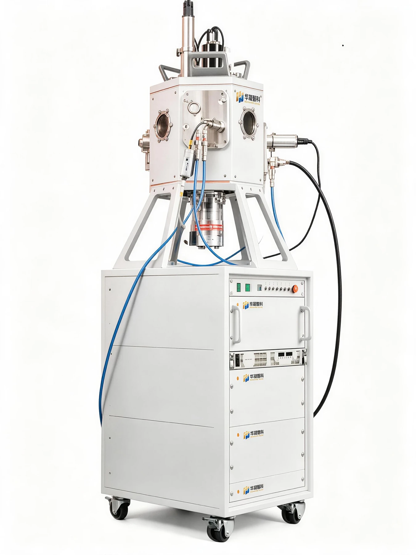
The HN-MS-EB-R-010 integrates magnetron sputtering and electron beam evaporation in a single ultra-high-vacuum research chamber. Designed for university laboratories, materials research institutes, and semiconductor research centers, the system supports thin-film research activities ranging from optical multilayer development to semiconductor device heterostructures.
Working Principle
A shared ultra-high-vacuum environment with independent magnetron sputtering and e-beam evaporation sources allows researchers to leverage the strengths of each technique within a single experiment. Sputtering excels at reactive deposition of stoichiometrically controlled compounds; evaporation delivers low-defect, high-purity films of refractory materials and compound semiconductors. Sequential and co-deposition modes are supported.
Core Advantages
- Broadest material and process coverage in a single research system
- Ultra-high-vacuum design with an ultimate pressure of ≤ 3 × 10⁻⁸ Torr
- Independent control of all source, substrate, and atmosphere parameters
- Multiple in-situ diagnostic integration ports
- Sequential and co-deposition capability
- Wide-range substrate heating from ambient to 1200 °C with in-situ annealing
- Integrated in-situ ion cleaning for substrate preparation
- Supports wafers up to 8 inches and small research samples or coupons
- Ion-beam-assisted deposition for enhanced film density and adhesion
- Advanced data acquisition and logging for research publication quality
Technical Specifications
| Chamber | φ600 mm partitioned research chamber |
|---|---|
| Standard Sources | 3 DC/RF magnetron targets and one 4-crucible electron-beam gun |
| Vacuum System | Ultra-high-vacuum system with independent zoned pumping; ultimate pressure ≤ 3 × 10⁻⁸ Torr |
| Control | Open process programming with local storage for more than 1,000 experiment recipes |
| Data System | Automatic process-data storage and Origin-compatible curve export |
| Integration | Reserved rapid vacuum sampling port for SEM/AFM integration |
| Temperature Control | Wide-range substrate temperature control from ambient to 1200 °C with in-situ annealing |
| Substrate Preparation | Integrated in-situ ion cleaning for substrate surface activation before deposition |
| Sample Compatibility | Wafers up to 8 inches and small research samples or coupons |
| Ion Assistance | Ion-beam-assisted deposition for enhanced film density and adhesion |
Specifications are representative. Final system parameters are defined during configuration. Contact our engineering team for detailed documentation.